

Electron Microscopy Room (EMR)
Phone:
+7-495-952-72-98
Address:
Russia, 119071, Moscow, Leninskij prosp., 33; room. 203, 305, 308
The Electron Microscopy Room (EMR) was created in 1959 under the leadership of N.P. Dmitrieva (DrSci.(Biol.)). From 1967 to 2008 a head of EMR was M.M. Kalashnikova (Ph.D.(Biol.)). From 2008 to 2018 – O.F. Chernova (DrSci.(Biol.)) supervised EMR. From 2019 to resent time – ÍÓÆÍÎ ÄÎÁÀÂÈÒÜ. Until 2008, the instrumental base of EMR was represented by transmission (Jeol JEM100C and Jeol JEM-100SX) (Jeol, Japan) and scanning (Jeol JSM-840 (Jeol, Japan) and Tescan Vega TS5130MM (Tescan, the Czech Republic)) electron microscopes. Nowadays only scanning electron microscopes function in EMR. Also, there is a light microscope LEICA DMR (Leica Microsystems, Germany), equipped by digital camera JVC 3 CCD C-MOUNT. In addition there is a full line of tools for biological samples preparation for scanning electron microscopy: Hitachi Critical Point Dryer HCP-1 (Hitachi, Japan) for critical point drying, S150A Sputter Coater (Edwards, United Kingdom) for conductive metal layer sputtering. The main tasks of EMR include technical assistance for researchers from different laboratories during preparation of samples, their investigation via electron microscopes and processing of received data. Microscopes of EMR are used in the different investigations, carried out by researchers of the Institute. The scanning electron microscopes are used for morphological investigation of almost all groups of organisms. A light microscope is commonly used for microphotographs obtaining with subsequent morphometric analysis and for investigation of morphological features of bird feathers. The obtained results are reflected in numerous Ph.D and DrSci. theses, monographs of the Institute staff, as well as in the bachelor and master theses of students performed under the supervision of the Institute staff
AREAS OF RESEARCH
- Cabinet microscopes are used in various studies carried out by the staff of the Institute.
- SEMs are used in the detailed study of the morphology of almost all groups of organisms.
- The light-optical microscope is widely used in obtaining micrographs for subsequent morphometric analysis, as well as for studying the features of the morphology of bird feathers.
- The results obtained are reflected in candidate and doctoral dissertations, monographs of the Institute staff, as well as term and diploma works of students, carried out under the guidance of the Institute staff.
INSTRUMENT BASE
The Institute's ability to solve a wide range of scientific problems at the modern level is determined by the use of the latest scientific and technical equipment for research. Scanning electron microscopy (SEM) is one of the most informative and versatile methods for studying biological (as well as industrial) objects. The versatility is expressed in the fact that there are several dozen accessories that can be installed on the column of a scanning electron microscope, and each of the accessories is used for its own purpose (obtaining images at high magnifications, local elements analysis, local phase analysis, etc.). The interchangeability of the attachments transforms the basic device into a powerful research complex. A scanning electron microscope is capable of examining samples of different sizes and shapes, the only limitation is that the sample must be placed in the microscope chamber (SEM with an inner chamber diameter of 230 mm is sufficient for typical Institute samples).
The scanning electron microscope TESCAN MIRA 3 LMH has the following advantages:
- Examination of samples in a wide range of magnifications from 2 × to 1,000,000 × with high resolution (passport microscope resolution 1.2 nm).
- Sample stage allows you to move samples along X, Y, Z;
- Tilting samples in the range from - 80 ° to + 80 °, rotating them by 360 °;
- All movements of the table are motorized and can be programmed, it is possible to reproduce previously saved coordinates;
- The presence of an electron gun with a field emission cathode in SEM (in contrast to the traditionally used tungsten cathodes or LaB6 cathodes) transfers SEM to a higher class of microscopes, all characteristics of which are significantly improved. For example, the high brightness of the electron beam (which is a thousand times higher than that of a classical SEM with a tungsten cathode) makes it possible to obtain saturated images with a good signal-to-noise ratio at high magnifications in a short time. The presence of an SEM with a field emission cathode becomes essential if, for example, samples with a fine surface structure (which are many biological objects) are studied at high magnifications. In these cases, more information about the sample can be obtained by lowering the accelerating voltage (HV) of the electron beam, and it is the SEM with a field emission cathode that makes the work at low HV efficient, without the need to find a compromise between lowering HV and image quality;
- Smooth change in magnification over the entire range from 2× to 1,000,000×, which allows one to study the general nature of the structure of the entire surface of an object at low magnifications and then study in detail selected local areas of the sample at higher magnifications. In this case, there is no need to develop special sighting methods characteristic of optical microscopes;
- TESCAN microscopes use the patented Wide Field OpticsTM technology, which, in particular, allows you to work in scanning mode with an extended depth of field, which is essential when studying surfaces with a developed relief. A large depth of field is the second
(after spatial resolution) significant advantage of SEM over optical microscopes. A typical SEM consists of an electro-optical column, an electronics unit and a control computer (sometimes the column and the electronics unit are combined).
All modern SEM images are generated immediately in digital format. Comparison of SEM with other common microscopic techniques can be conventionally imagined as follows, Fig. 1: a) optical microscopy - color images at low and medium magnifications; b) scanning electron microscopy - black-and-white pictures at low, medium and high magnifications, objects in the pictures look three-dimensional; c) transmission electron microscopy - black-and-white images at high and very high magnifications, objects in the images look flat.
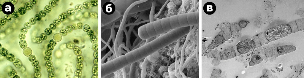
Figure 1. Typical images: a - optical microscope; b - scanning electron microscope; c - transmission electron microscope.
The SEM column contains, from top to bottom: an electron gun, where an electron beam is formed; a set of electromagnetic coils that focus this beam; sample chamber, where samples are placed. The SEM name contains the word “scanning”, because when constructing SEM images, a finely focused electron beam scans the sample surface; paints the pattern point by point. The SEM image is formed following the movement of the electron beam sequentially in time, pixel by pixel. For comparison, photographing on photographic film is a parallel method of imaging, because all the grains of the photographic film are illuminated simultaneously. The smaller the electron beam diameter, the better spatial resolution can be achieved. Typical electron beam diameter is <10 nm, although this value strongly depends on the design and settings of the SEM. When the focused electron beam interacts with the sample surface, many response signals are generated. Each type of signal is especially sensitive to a certain property of the sample; to register each type of signal, its own detector design is required. Sample properties that can be observed in SEM are: sample surface topography, compositional contrast, composition of microcomponents, orientational contrast, as well as more subtle features that are more difficult to detect, such as differences in conductivity, magnetic properties, crystal structure defects, presence trace impurities;
- The original 3D Beam technology, patented by TESCAN, makes it possible to work with "live" stereo images of micro- and nano-objects in real time, which is indispensable when analyzing samples with complex topography.
- Image pixel size up to 16,384 × 16384 pixels, 11 image sizes to choose from. Essentially when analyzing the morphological properties of many small objects in one frame with good statistical reliability;
- Other technical features: upgraded electronics and ultra-fast scanning system (from 20 ns / pixel) with compensation for static and dynamic aberrations; flicker-free digital image; the absence of mechanically centered elements in the microscope column (an additional electromagnetic lens works as a device for changing the aperture, which is easier to control compared to mechanical changing the apertures).
There are several attachments to TESCAN MIRA 3 LMH EMS:
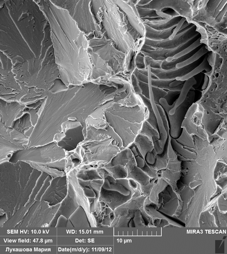
- A classic detector for obtaining electronic images - SE (secondary electrons) detector. The secondary electron signal is sensitive to the surface relief of the sample; therefore, the SE detector is used when studying the surface morphology. For example, an SE detector is needed to observe biological samples of fractures, pores, microrelief and surface symbionts, to understand the general appearance of the samples (Fig. 2).
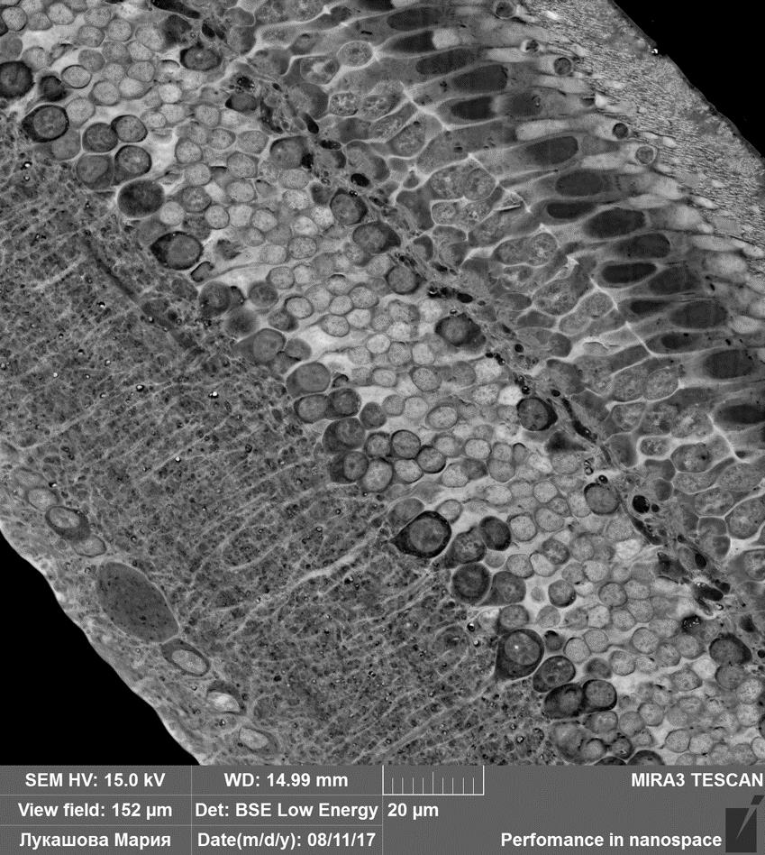
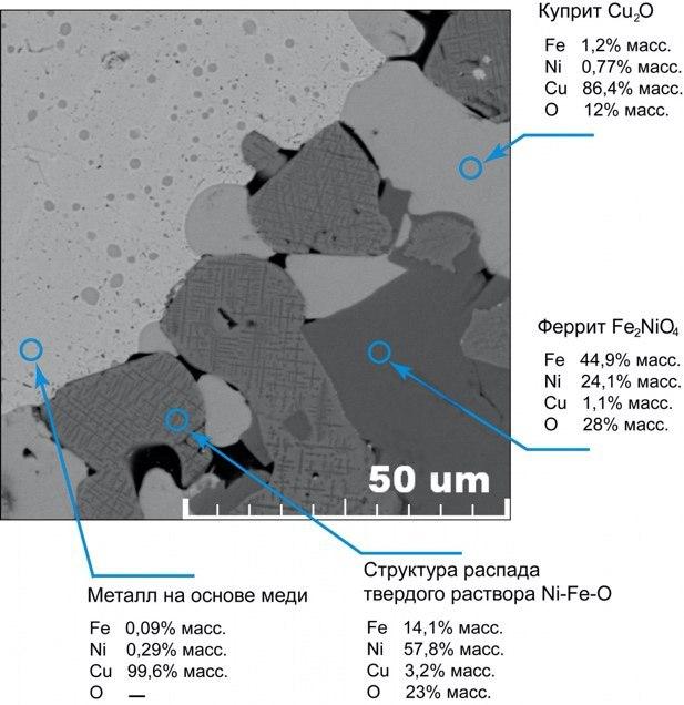
- A detector for obtaining electronic images, in which objects of different composition are presented in different shades - a BSE (back scattered electrons) detector. The reflected electron signal is sensitive to compositional contrast, i.e. sample components with different compositions will have different shades in grayscale in BSE images (Fig. 3). This allows to visualize the difference in composition between the constituents of the sample.
- The EDS Aztec One X-act energy dispersive spectroscopy (energy dispersive spectroscopy) system, which performs elemental analysis of microinclusions with a sensitivity of <0.1% wt. This is the next step after visualizing the difference in compositions on BSE images, namely, determining these compositions. The EDS detector allows to determine the elemental composition of microinclusions and microparticles. It is the elemental composition that is analyzed, and not chemical, molecular, mineral, isotopic, or anything else. Fig. 4 shows an example of a local analysis of compositions using an EDS detector; an image from a backscattered electron detector is used as a substrate. The EDS detector determines the compositions locally, separately for each micro-component of the sample, which is sometimes more important than the accuracy of the analysis. For example, using an EDS detector, it is possible to establish what elements a non-metallic inclusion in a fracture center consists of. The composition of the sample area where the narrow electron beam is directed at the moment is determined. Another advantage of EDS analysis is that this type of analysis does not require any reagents. Even the presence of standard samples for the EDS method is an option that clarifies the result, and not a necessity.
CEM Regulations >>
Rules of work in CEM >>
Official duties of the CEM technician >>
CABINET HEAD OFFICIAL

Khatsaeva Raisa Musaevna. Doctor of Biological Sciences, Leading Researcher at the Institute of Ecology and Evolution. A.N. Severtsov RAS, head. cabinet of electron microscopy. More than 90 scientific works, including teaching aids, atlases and monographs.
Brief description of scientific activity.
Elucidation of the mechanisms of morphological adaptations of the digestive organs of vertebrates (mammals and birds) at all levels of structural organization associated with the specifics of their nutrition and maintenance.
Revealing the principles of compensation of functions at different levels of the structural organization between the digestive organs and within them; determination of the direction of development of the type of digestion in closely related wild and domestic species Caprinae and Bovinae in phylogeny; determination of morphological and functional criteria of the digestive system at all levels of structural organization for the classification of Caprinae and Bovinae by type of nutrition.
Elucidation of the mechanisms of morphological adaptations of the digestive organs of vertebrates at all levels of structural organization, associated with the specifics of nutrition and maintenance. Ruminant digestive organs, adaptation, nutritional specifics.
Laboratory staff
| Surname | Name | Patronym | Position | Academic degree |
| Khatsayeva | Raisa | Musaevna | Cabinet head, leading researcher | Ph.d |
| Metelev | Sergey | Ivanovich | Electronic engineer | |
| Nekrasov | Alexei | Nikolaevich | Electronic engineer | |
| Neretina | Anna | Nikolaevna | Electronic engineer |